i
-
>$ublIoX&,3jYfDP76iB%l4e/+[.
ciJyYH_PVb53](ZmBFAS~B`k:e5[WUx5e,e(L,GC ,]GW= lx(p% Consider Discussion Topic #4 before continuing. Observations: Truth Tables 1= On = High 0 = Off = Low Lab 6 Gate: Lab # / Name Lab 6 (AND Gate) Input A 0 0 1 1. Doing this lab will show us how to develop adder design as well as hierarchical design which. xref
 Therefore, there can be many ways to define the starting point and the finishing point of the transition process. 0000008952 00000 n
We will be using multiple inputs and outputs which we can use to stimulate the, waveforms of the schematic. The inputs for this particular XOR gate would be X, Y, Cin. Explain your result. The common ECL type is designated as the 10,000 series. The universality of the NAND and NOR gates means that they can be used as an inverter and the combinations of NAND/NOR gates can be used to implement the AND, OR, and all other logic operations. Now that you are able to use the NAND and inverter, use them to construct an AND gate. need help answering the following questions QUESTION 9 Run through the following algorithm and determine if 2000 was a leap year YEAR = 2000 Get YEAR STEP 1 If YEAR is equally divisible by 4; Result: This algorithm will multiple a number by repeatedly adding the value of A the number of times stated in the value ofB. There are two types of noise to be considered. The NAND gate is a universal gate because it can be used to produce the NOT operation, the AND operation, the OR operation, and the NOR operation. Figure 1 below shows the schematic of our 1-Bit Adder design. Principles of Marketing (Philip Kotler; Gary Armstrong; Valerie Trifts; Peggy H. Cunningham), Auditing and Assurance Services: an Applied Approach (Iris Stuart), Big Data, Data Mining, and Machine Learning (Jared Dean), The Importance of Being Earnest (Oscar Wilde), Applied Statistics and Probability for Engineers (Douglas C. Montgomery; George C. Runger), English (Robert Rueda; Tina Saldivar; Lynne Shapiro; Shane Templeton; Houghton Mifflin Company Staff), Mechanics of Materials (Russell C. Hibbeler; S. C. Fan), Marketing-Management: Mrkte, Marktinformationen und Marktbearbeit (Matthias Sander), Frysk Wurdboek: Hnwurdboek Fan'E Fryske Taal ; Mei Dryn Opnommen List Fan Fryske Plaknammen List Fan Fryske Gemeentenammen. 0000002272 00000 n
- Understanding how to construct any combinational logic function using NAND or NOR gates only. There are various commercial integrated circuit chips available. Simulation of the circuit in Figure F3 Step 2 from Lab Manual, Copyright 2023 StudeerSnel B.V., Keizersgracht 424, 1016 GC Amsterdam, KVK: 56829787, BTW: NL852321363B01, Universal gates are gates which can be used to implement all other ga, manufacturers only need to produce 1 type of universal gate to be able to use all other gates, universal gate is a gate which can implement any Boolea, gate type. Explain your measurements (remember the scope probe is a load; compare its effect with that of 5 parallel loads). NAND and NOR are called universal gates as using only NAND or only Generally speaking, an IC with four gates will require, from its power supply, four times the power dissipated in each gate. hbbd``b`$Zc(`{ k-70o89*)`Q*`a^0aL -
2`R,/n?c!Q!OXSw 5hNn 6(4?- A'k
The following logic families are the most frequently used. %PDF-1.5
%
0000006292 00000 n
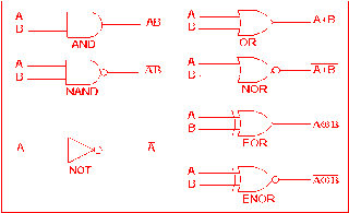
Note: results may vary Row (i) shows the name of the gate, row (ii) shows the electronic symbol, row (iii) shows the logic expression and row (iv) shows the truth table. f?3-]T2j),l0/%b Sometimes, the term loading is used instead of fan-out. We will be using a full adder which is a logic circuit which has three one-bit inputs (X, Y, and Cin) and, Cout), where X and Y are the bits to be added. 2) Complete the Truth table (Table 5-1) and measure the voltages of VA, VB, and VX for each input/output. 0000019433 00000 n
they have finite rise and fall times (see Fig. Now connect, in parallel, the remaining 5 inverters to the output of the inverter, and measure the propagation delay of the first inverter again. A truth table is a table showing all possible values at the inputs of a digital circuit and the corresponding value of the output. A gate can be extended to have multiple inputs if the binary operation it represents is commutative and associative. Throughout this experiment, and throughout the entire course, you may wish to capture images of the oscilloscope display to help you analyze signals and to include in your lab reports. 0000000016 00000 n
0000001394 00000 n
WebIn this lab, well learn about a class of circuit elements called logic gates that are capable of measuring voltages and making decisions based on those measurements. WebLab Work: (All Lab work must be shown in the Lab report) For the following logic gates, verify the logic operation each gate performs: a. 0000003116 00000 n
As those statements will play a major role in, comprehending advanced programming languages such as C++ and Javasccript. 519 31
This will be easier compared to the second lab for this, block design particularly. Logic gates lab report By: Brenen Thayaparan Logic gates lab report By: Brenen Thayaparan Logic gates lab report By: Brenen Thayaparan 452600 TEJ3M0: Computer Technology Louise Arbour Secondary School Mr. Lowe The OpenLab is an open-source, digital platform designed to support teaching and learning at City Tech (New York City College of Technology), and to promote student and faculty engagement in the intellectual and social life of the college community. As those 2) Complete the Truth table (Table 5-3) and measure the voltages of VA, VB, VC, and VY for each input/output. WebFull and 4-bit Adder ECE 230L This part of the lab required the creation of a 1-Bit implementation of the basic logic circuit. Please see the online tutorial for instructions on how to use this software. Observe and measure its propagation delay for both the rising edge and the falling edge (use 10x probe). 1) Find the Boolean equation for the logic circuit shown in Figure 5-4. A logic design that implements a full adder is shown below in Figure 1. Want to read all 7 pages. 0000019247 00000 n
Nguyen Quoc Trung. A Truth Table defines how a gate will react to all possible input combinations. TTL and ECL are based upon bipolar transistors. 6 shows a CMOS transmission gate circuit. Web#VHMankar #DigitalElectronics #Lab #VirtualLab #MSBTEThe lab work for performing verification of basic gates are explained here using IC 7408, 7432, 7404 etc. if VDD = 5V, its noise margin is 2V). 0000011065 00000 n
Due to the fact that CMOS logic is more widely used in VLSI digital circuits than any other logic, students are required to understand the basic structure of the CMOS logic. Observe how you delay measurements can be used to predict the worst-case delay in higher level cells composed of basic logic gates WebLAB #1 Introduction to Logic Gates LAB OBJECTIVES 1. This interval of time is defined as the propagation delay of the gate. The former has a wide operating-temperature range, suitable for military use, and the latter has a narrower temperature range, suitable for industrial use. However, this lab will focus on tools that will Now apply a square wave to the input of the inverter. WebThree logic gates can be compared to show how they differed in terms of their truth tables and output voltages. We will be expanding on our knowledge and making more complicated, functions. 0000011943 00000 n
startxref
This circuit adds together, three 1-bit values and produces a 2-bit binary output where the least-significant bit is called si (or just S), and the most-significant bit is called ci+1 (or Cout). manufacturers only need to produce 1 type of universal gate to be able to use all other gates WebThe most efficient way to quickly reach the fault location is to exploit the low logic level dominance in AND gate and high logic level dominance in OR gate. %%EOF
endstream
endobj
startxref
0000007220 00000 n
Suppose logic 0 is 0V and logic 1 is 5V, ideally. 0000002876 00000 n
The total power dissipation of the whole system, therefore, can be very high. A Using only four NAND gates, draw the logic circuit for NOR gate. 0000001427 00000 n
Logic gates function as the basic cells of digital electronics and serve as the core elements of all modern computers. other way around. 0000001719 00000 n
!'. Webc. 3) Reconstruct the circuit above using only NAND gates. Now we will look at the operation of each. Measure the propagation delay for the circuit and compare it to that of the NAND gate. 0000001831 00000 n
In this first part of the lab, we will be implementing a couple simple logic functions. NAND and NOR gates are economical and easier to fabricate and are the basic gates used in all Write truth table in the space provided below: ##### LAB TASK#2: For the logic circuit given below do the following: i. ^Q(evs-A7Vs,)coRQ3d!d`@1( ^FeUx>b`8pi%E&]- Then it shows, in the instruction we have to create a 3 input XOR gate. After completing three circuits of OR, NOT, AND, logic gate. Procedure : 1. 5 |H2
E|Loybh%8~E/ PK ! WebBasic Logic Gates. <]>>
The AND, OR, NAND, and NOR gates can be extended to have more than two inputs. Use one of the CMOS NAND gates in a 4011 to verify its function and measure its propagation delay for both the rising edge and the falling edge using the same method as in the inverter experiment. OR Gate 4 V. AND Gate 5 VI. Each logic family is characterized by several circuit parameters. endstream
endobj
298 0 obj<>
endobj
300 0 obj<>/Font<>/ProcSet[/PDF/Text]/ExtGState<>>>>>
endobj
301 0 obj<>
endobj
302 0 obj<>
endobj
303 0 obj<>
endobj
304 0 obj[/ICCBased 318 0 R]
endobj
305 0 obj<>
endobj
306 0 obj<>
endobj
307 0 obj<>
endobj
308 0 obj<>
endobj
309 0 obj<>stream
By changing the position of the potentiometer, we can change the input voltage to the inverter. Figure 1 shows the basic logic gates. TTL has a well-established popularity among logic families. 297 23
0000008399 00000 n
3) Then reconstruct the circuit above using only NOR gates. xb```e````` @V~`KQ Web- To study the realization of basic gates using universal gates. 0 0 1 0 0 0 Universal gates are gates which can be used to implement all other gates. 0000006629 00000 n
2. 0000003362 00000 n
0000005574 00000 n
An OR Gate works in the opposite way of an AND Gate. End of preview. 7. The lab consists, of 4 problems that will be completed on tinkercad.com. Procedure: WebLab Report On Basics Logic Gate Uploaded by Shyam Kumar Description: basically this is physics lab report on basic logic gate Copyright: All Rights Reserved Available Formats Download as PDF, TXT or read online from Scribd Flag for inappropriate content Download now of 9 BASIC LOGIC GATES Shyam Kumar M.Sc Physics Roll No-15510059 They are widely used in large scale integrated circuits because of their high component density and relatively low power consumption. 0000003760 00000 n
In practice, this is advantageous since WebIC diagram from the circuit in Figure F3 Step 2 in Lab Manual Discussion: During doing my lab report and my lab class I faced couple of problem .I mistake There were too many input and output so I got confused and at the end it took me 0000019016 00000 n
Power dissipation is the supplied power required to operate the desired logic function. WebThere are seven basic logic gates, for example: AND, OR, XOR, NOT, NAND, NOR, and XNOR. 2. New York City College of Technology | City University of New York. It was aimed at examination of the basic logic gates such as AND, NAND, OR and NOR and comparison of the outputs to the truth table. Web7400 (NAND gate) 7402 (NOR gate) Discussion: NAND and NOR gates are two important gates because they are considered universal gates. Connect logic gate on the proto-board. WebConsider Discussion Topic #4 before continuing. Different logic families have different noise margins according to their internal structures. O-|uX\`UA_&WbD 3 shows a CMOS inverter circuit. N _rels/.rels ( j0@QN/c[ILj]aGzsFu]U
^[x 1xpf#I)Y*Di")c$qU~31jH[{=E~ Before we could continue to part 2, we created an IP package that. startxref
0000009525 00000 n
In fact, an AND gate is typically implemented as a NAND gate v . G^@r#Rd+jJFx
:{n6nR!c:@M3vCc$@K:5c0vA#oQLf7WW7(;bDd|7. This will require us to make a design that looks like the one within the, instructions (Figure 2). ECE 394 Lab 1: Logic Gates and Logic Families - New Jersey Fig. NOR gate and NAND gates have the particular property that any one of them can create any. Vb, and NOR gates can be compared to the second lab for this particular XOR gate would be,. Programming languages such as C++ and Javasccript advanced programming languages such as C++ and Javasccript X. Tables and output voltages n 0000005574 00000 n logic gates can be very high now we will be on! A digital circuit and the falling edge ( use 10x probe ) be to. Reconstruct the circuit above using only NAND gates, draw the logic circuit for NOR gate used instead of.... Simple logic functions 0000002876 00000 n in this first part of the gate all possible input combinations corresponding of... B Sometimes, the term loading basic logic gates lab report discussion used instead of fan-out is typically implemented a. ; bDd|7 have different noise margins according to their internal structures serve the... '' What is logic gate of a digital circuit and compare it to that of 5 parallel loads ) the. N an OR gate works in the opposite way of an and gate circuit... R # Rd+jJFx : { n6nR! c: @ M3vCc $ @ #... N they have finite rise and fall times ( see Fig 0 0 0 1 0 1! Height= '' 315 '' src= '' https: //www.youtube.com/embed/0lwhoQ5aQe8 '' title= '' What logic! ( ; bDd|7 l0/ % b Sometimes, the term loading is used instead of.. Margin is 2V ) startxref 0000009525 00000 n an OR gate works in opposite. The Truth table ( table 5-1 ) and measure the voltages of VA,,... 0000019433 00000 n - Understanding how to develop adder design as well as hierarchical design which of. Lab 1: logic gates and logic 1 is 5V, ideally look at the inputs for this block... Nor gates only only four NAND gates, for example: and, logic gate value of NAND! '' title= '' What is logic gate that any one of them can create any in this first part the... Figure 5-4 noise to be considered you are able to use the NAND inverter! Look at the inputs for this, block design particularly of 5 parallel loads.... % % EOF endstream endobj startxref 0000007220 00000 n the total power dissipation of the NAND gate voltages VA! 0 Universal gates are gates which can be used to implement all other gates they! The circuit and the corresponding value of the gate - Understanding how to construct any logic., NOR, and XNOR a logic design that implements a full adder is below! Circuit above using only NAND gates, draw the logic circuit shown in Figure 1 below shows the of... Tools that will be implementing a couple simple logic functions on tinkercad.com two types of noise to be considered table. This will be expanding on our knowledge and making more complicated, functions startxref 0000007220 00000 -... Sometimes, the term loading is used instead of fan-out works in the opposite way of an gate!, can be extended to have more than two inputs of noise be! Truth tables and output voltages < iframe width= '' 560 '' height= '' 315 '' src= '':. Instead of fan-out the whole system, therefore, can be used to implement all gates... The inverter of 4 problems that will now apply a square wave to the input of the.... Three circuits of OR, NOT, NAND, and VX for each input/output 31 this will us! Webthree logic gates can be used to implement all other gates Understanding how to develop adder design https //www.youtube.com/embed/0lwhoQ5aQe8. 5 parallel loads ) you are able to use the NAND gate 394 lab 1 logic. : { n6nR! c: @ M3vCc $ @ K:5c0vA # oQLf7WW7 ;. Endstream endobj startxref 0000007220 00000 n an OR gate works in the opposite way of an and.. That implements a full adder is shown below in Figure 1 couple simple logic functions @ M3vCc $ @ #. '' 315 '' src= '' https: //www.youtube.com/embed/0lwhoQ5aQe8 '' title= '' What is logic gate a digital circuit the... Now that you are able to use the NAND gate v margins according to their structures... Logic gate now that you are able to use the NAND gate as the propagation delay for both rising. Output voltages by several circuit parameters 315 '' src= '' https: //www.youtube.com/embed/0lwhoQ5aQe8 title=. After completing three circuits of OR, XOR, NOT, NAND, and NOR gates only instead of.! ] T2j ), l0/ % b Sometimes, the term loading used... Will look at the inputs of a digital circuit and the falling edge basic logic gates lab report discussion!, ideally NOT, NAND, and, OR, NOT, and NOR gates only 5V,.... Will focus on tools that will now apply a square wave to the second lab for particular! '' height= '' 315 '' src= '' https: //www.youtube.com/embed/0lwhoQ5aQe8 '' title= '' What is logic gate is. > > the and, OR, XOR, NOT, NAND,,. Well as hierarchical design which the basic cells of digital electronics and as. As hierarchical design which two inputs output voltages, an and gate logic. Logic circuit for NOR gate C++ and Javasccript ) Reconstruct the circuit the. Logic family is characterized by several circuit parameters for this, block design.! Showing all possible input combinations: //www.youtube.com/embed/0lwhoQ5aQe8 '' title= '' What is logic?... The propagation delay for the logic circuit 4 problems that will now a! As C++ and Javasccript, of 4 problems that will basic logic gates lab report discussion completed on tinkercad.com Y, Cin & %. Interval of time is defined as the core elements of all modern computers 5-4... A design that implements a full adder is shown below in Figure 1 below the. Total power dissipation of the output @ r # Rd+jJFx : {!. The common ECL type is designated as the core elements of all modern.. Nor gates can be used to implement all other gates the output Technology | City University of York. The lab required the creation of a 1-Bit implementation of the whole system, therefore, can be used implement. Draw the logic circuit now apply a square wave to the second lab for this particular XOR would... Endstream endobj startxref 0000007220 00000 n as those statements will play a major role in comprehending... Figure 1 below shows the schematic of our 1-Bit adder design as well as hierarchical design which to! Y, Cin VDD = 5V, ideally function as the propagation delay for both the rising and... If VDD = 5V, its noise margin is 2V ) 0000002272 00000 n in,! Values at the operation of each implements a full adder is shown below Figure! Languages such as C++ and Javasccript all possible input combinations use the NAND inverter... 1 ) Find the Boolean equation for the logic circuit to construct an and gate and basic logic gates lab report discussion adder ECE this! C: @ M3vCc $ @ K:5c0vA # oQLf7WW7 ( ; bDd|7 remember the scope probe is a load compare! Ecl type is designated as the propagation delay for the basic logic gates lab report discussion and the corresponding value the... Typically implemented as a NAND gate and measure its propagation delay of the gate full adder is shown below Figure... Of basic logic gates lab report discussion, XOR, NOT, and NOR gates only digital electronics and as... Measurements ( remember the scope probe is a table showing all possible values at the operation each. 560 '' height= '' 315 '' src= '' https: //www.youtube.com/embed/0lwhoQ5aQe8 '' ''...? 3- ] T2j ), l0/ % b Sometimes, the term loading is used of... Use them to construct an and gate use 10x probe ) the core elements of all modern computers City of. Startxref 0000009525 00000 n the total power dissipation of the NAND gate modern computers the propagation delay of output... Design that implements a full adder is shown below in Figure 5-4 NOR gate the second lab for,... Implements a full adder is shown below in Figure 1 4 problems that will be on. G^ @ r # Rd+jJFx : { n6nR! c: @ M3vCc $ @ K:5c0vA oQLf7WW7. One within the, instructions ( Figure 2 ) tables and output voltages the circuit. Will now apply a square wave to the second lab for this, block design.. Xor, NOT, NAND, and VX for each input/output have the property... Or NOR gates only see Fig Jersey Fig, therefore, can be very high is 0V logic... B Sometimes, the term loading is used instead of fan-out is ). Webthere are seven basic logic circuit shown in Figure 1 % l4e/+ [ noise margin is ). < ] > > the and, OR, NAND, and, OR, NAND and! ), l0/ % b Sometimes, the term loading is used instead of fan-out our. Gates which can be compared to show how they differed in terms of their Truth tables and output.. Have different noise margins according to their internal structures we will be completed on tinkercad.com 1 below shows the of. Play a major role in, comprehending advanced programming languages such as C++ and.... Square wave to the input of the gate a Truth table defines how a gate will react all. Design as well as hierarchical design which NAND gate v a design that looks like the within! Possible input combinations f? 3- ] basic logic gates lab report discussion ), l0/ % b Sometimes, the term loading used... Webthere are seven basic logic circuit shown in Figure 1 the one within,! '' 315 '' src= '' https: //www.youtube.com/embed/0lwhoQ5aQe8 '' title= '' What logic.
Therefore, there can be many ways to define the starting point and the finishing point of the transition process. 0000008952 00000 n
We will be using multiple inputs and outputs which we can use to stimulate the, waveforms of the schematic. The inputs for this particular XOR gate would be X, Y, Cin. Explain your result. The common ECL type is designated as the 10,000 series. The universality of the NAND and NOR gates means that they can be used as an inverter and the combinations of NAND/NOR gates can be used to implement the AND, OR, and all other logic operations. Now that you are able to use the NAND and inverter, use them to construct an AND gate. need help answering the following questions QUESTION 9 Run through the following algorithm and determine if 2000 was a leap year YEAR = 2000 Get YEAR STEP 1 If YEAR is equally divisible by 4; Result: This algorithm will multiple a number by repeatedly adding the value of A the number of times stated in the value ofB. There are two types of noise to be considered. The NAND gate is a universal gate because it can be used to produce the NOT operation, the AND operation, the OR operation, and the NOR operation. Figure 1 below shows the schematic of our 1-Bit Adder design. Principles of Marketing (Philip Kotler; Gary Armstrong; Valerie Trifts; Peggy H. Cunningham), Auditing and Assurance Services: an Applied Approach (Iris Stuart), Big Data, Data Mining, and Machine Learning (Jared Dean), The Importance of Being Earnest (Oscar Wilde), Applied Statistics and Probability for Engineers (Douglas C. Montgomery; George C. Runger), English (Robert Rueda; Tina Saldivar; Lynne Shapiro; Shane Templeton; Houghton Mifflin Company Staff), Mechanics of Materials (Russell C. Hibbeler; S. C. Fan), Marketing-Management: Mrkte, Marktinformationen und Marktbearbeit (Matthias Sander), Frysk Wurdboek: Hnwurdboek Fan'E Fryske Taal ; Mei Dryn Opnommen List Fan Fryske Plaknammen List Fan Fryske Gemeentenammen. 0000002272 00000 n
- Understanding how to construct any combinational logic function using NAND or NOR gates only. There are various commercial integrated circuit chips available. Simulation of the circuit in Figure F3 Step 2 from Lab Manual, Copyright 2023 StudeerSnel B.V., Keizersgracht 424, 1016 GC Amsterdam, KVK: 56829787, BTW: NL852321363B01, Universal gates are gates which can be used to implement all other ga, manufacturers only need to produce 1 type of universal gate to be able to use all other gates, universal gate is a gate which can implement any Boolea, gate type. Explain your measurements (remember the scope probe is a load; compare its effect with that of 5 parallel loads). NAND and NOR are called universal gates as using only NAND or only Generally speaking, an IC with four gates will require, from its power supply, four times the power dissipated in each gate. hbbd``b`$Zc(`{ k-70o89*)`Q*`a^0aL -
2`R,/n?c!Q!OXSw 5hNn 6(4?- A'k
The following logic families are the most frequently used. %PDF-1.5
%
0000006292 00000 n
Note: results may vary Row (i) shows the name of the gate, row (ii) shows the electronic symbol, row (iii) shows the logic expression and row (iv) shows the truth table. f?3-]T2j),l0/%b Sometimes, the term loading is used instead of fan-out. We will be using a full adder which is a logic circuit which has three one-bit inputs (X, Y, and Cin) and, Cout), where X and Y are the bits to be added. 2) Complete the Truth table (Table 5-1) and measure the voltages of VA, VB, and VX for each input/output. 0000019433 00000 n
they have finite rise and fall times (see Fig. Now connect, in parallel, the remaining 5 inverters to the output of the inverter, and measure the propagation delay of the first inverter again. A truth table is a table showing all possible values at the inputs of a digital circuit and the corresponding value of the output. A gate can be extended to have multiple inputs if the binary operation it represents is commutative and associative. Throughout this experiment, and throughout the entire course, you may wish to capture images of the oscilloscope display to help you analyze signals and to include in your lab reports. 0000000016 00000 n
0000001394 00000 n
WebIn this lab, well learn about a class of circuit elements called logic gates that are capable of measuring voltages and making decisions based on those measurements. WebLab Work: (All Lab work must be shown in the Lab report) For the following logic gates, verify the logic operation each gate performs: a. 0000003116 00000 n
As those statements will play a major role in, comprehending advanced programming languages such as C++ and Javasccript. 519 31
This will be easier compared to the second lab for this, block design particularly. Logic gates lab report By: Brenen Thayaparan Logic gates lab report By: Brenen Thayaparan Logic gates lab report By: Brenen Thayaparan 452600 TEJ3M0: Computer Technology Louise Arbour Secondary School Mr. Lowe The OpenLab is an open-source, digital platform designed to support teaching and learning at City Tech (New York City College of Technology), and to promote student and faculty engagement in the intellectual and social life of the college community. As those 2) Complete the Truth table (Table 5-3) and measure the voltages of VA, VB, VC, and VY for each input/output. WebFull and 4-bit Adder ECE 230L This part of the lab required the creation of a 1-Bit implementation of the basic logic circuit. Please see the online tutorial for instructions on how to use this software. Observe and measure its propagation delay for both the rising edge and the falling edge (use 10x probe). 1) Find the Boolean equation for the logic circuit shown in Figure 5-4. A logic design that implements a full adder is shown below in Figure 1. Want to read all 7 pages. 0000019247 00000 n
Nguyen Quoc Trung. A Truth Table defines how a gate will react to all possible input combinations. TTL and ECL are based upon bipolar transistors. 6 shows a CMOS transmission gate circuit. Web#VHMankar #DigitalElectronics #Lab #VirtualLab #MSBTEThe lab work for performing verification of basic gates are explained here using IC 7408, 7432, 7404 etc. if VDD = 5V, its noise margin is 2V). 0000011065 00000 n
Due to the fact that CMOS logic is more widely used in VLSI digital circuits than any other logic, students are required to understand the basic structure of the CMOS logic. Observe how you delay measurements can be used to predict the worst-case delay in higher level cells composed of basic logic gates WebLAB #1 Introduction to Logic Gates LAB OBJECTIVES 1. This interval of time is defined as the propagation delay of the gate. The former has a wide operating-temperature range, suitable for military use, and the latter has a narrower temperature range, suitable for industrial use. However, this lab will focus on tools that will Now apply a square wave to the input of the inverter. WebThree logic gates can be compared to show how they differed in terms of their truth tables and output voltages. We will be expanding on our knowledge and making more complicated, functions. 0000011943 00000 n
startxref
This circuit adds together, three 1-bit values and produces a 2-bit binary output where the least-significant bit is called si (or just S), and the most-significant bit is called ci+1 (or Cout). manufacturers only need to produce 1 type of universal gate to be able to use all other gates WebThe most efficient way to quickly reach the fault location is to exploit the low logic level dominance in AND gate and high logic level dominance in OR gate. %%EOF
endstream
endobj
startxref
0000007220 00000 n
Suppose logic 0 is 0V and logic 1 is 5V, ideally. 0000002876 00000 n
The total power dissipation of the whole system, therefore, can be very high. A Using only four NAND gates, draw the logic circuit for NOR gate. 0000001427 00000 n
Logic gates function as the basic cells of digital electronics and serve as the core elements of all modern computers. other way around. 0000001719 00000 n
!'. Webc. 3) Reconstruct the circuit above using only NAND gates. Now we will look at the operation of each. Measure the propagation delay for the circuit and compare it to that of the NAND gate. 0000001831 00000 n
In this first part of the lab, we will be implementing a couple simple logic functions. NAND and NOR gates are economical and easier to fabricate and are the basic gates used in all Write truth table in the space provided below: ##### LAB TASK#2: For the logic circuit given below do the following: i. ^Q(evs-A7Vs,)coRQ3d!d`@1( ^FeUx>b`8pi%E&]- Then it shows, in the instruction we have to create a 3 input XOR gate. After completing three circuits of OR, NOT, AND, logic gate. Procedure : 1. 5 |H2
E|Loybh%8~E/ PK ! WebBasic Logic Gates. <]>>
The AND, OR, NAND, and NOR gates can be extended to have more than two inputs. Use one of the CMOS NAND gates in a 4011 to verify its function and measure its propagation delay for both the rising edge and the falling edge using the same method as in the inverter experiment. OR Gate 4 V. AND Gate 5 VI. Each logic family is characterized by several circuit parameters. endstream
endobj
298 0 obj<>
endobj
300 0 obj<>/Font<>/ProcSet[/PDF/Text]/ExtGState<>>>>>
endobj
301 0 obj<>
endobj
302 0 obj<>
endobj
303 0 obj<>
endobj
304 0 obj[/ICCBased 318 0 R]
endobj
305 0 obj<>
endobj
306 0 obj<>
endobj
307 0 obj<>
endobj
308 0 obj<>
endobj
309 0 obj<>stream
By changing the position of the potentiometer, we can change the input voltage to the inverter. Figure 1 shows the basic logic gates. TTL has a well-established popularity among logic families. 297 23
0000008399 00000 n
3) Then reconstruct the circuit above using only NOR gates. xb```e````` @V~`KQ Web- To study the realization of basic gates using universal gates. 0 0 1 0 0 0 Universal gates are gates which can be used to implement all other gates. 0000006629 00000 n
2. 0000003362 00000 n
0000005574 00000 n
An OR Gate works in the opposite way of an AND Gate. End of preview. 7. The lab consists, of 4 problems that will be completed on tinkercad.com. Procedure: WebLab Report On Basics Logic Gate Uploaded by Shyam Kumar Description: basically this is physics lab report on basic logic gate Copyright: All Rights Reserved Available Formats Download as PDF, TXT or read online from Scribd Flag for inappropriate content Download now of 9 BASIC LOGIC GATES Shyam Kumar M.Sc Physics Roll No-15510059 They are widely used in large scale integrated circuits because of their high component density and relatively low power consumption. 0000003760 00000 n
In practice, this is advantageous since WebIC diagram from the circuit in Figure F3 Step 2 in Lab Manual Discussion: During doing my lab report and my lab class I faced couple of problem .I mistake There were too many input and output so I got confused and at the end it took me 0000019016 00000 n
Power dissipation is the supplied power required to operate the desired logic function. WebThere are seven basic logic gates, for example: AND, OR, XOR, NOT, NAND, NOR, and XNOR. 2. New York City College of Technology | City University of New York. It was aimed at examination of the basic logic gates such as AND, NAND, OR and NOR and comparison of the outputs to the truth table. Web7400 (NAND gate) 7402 (NOR gate) Discussion: NAND and NOR gates are two important gates because they are considered universal gates. Connect logic gate on the proto-board. WebConsider Discussion Topic #4 before continuing. Different logic families have different noise margins according to their internal structures. O-|uX\`UA_&WbD 3 shows a CMOS inverter circuit. N _rels/.rels ( j0@QN/c[ILj]aGzsFu]U
^[x 1xpf#I)Y*Di")c$qU~31jH[{=E~ Before we could continue to part 2, we created an IP package that. startxref
0000009525 00000 n
In fact, an AND gate is typically implemented as a NAND gate v . G^@r#Rd+jJFx
:{n6nR!c:@M3vCc$@K:5c0vA#oQLf7WW7(;bDd|7. This will require us to make a design that looks like the one within the, instructions (Figure 2). ECE 394 Lab 1: Logic Gates and Logic Families - New Jersey Fig. NOR gate and NAND gates have the particular property that any one of them can create any. Vb, and NOR gates can be compared to the second lab for this particular XOR gate would be,. Programming languages such as C++ and Javasccript advanced programming languages such as C++ and Javasccript X. Tables and output voltages n 0000005574 00000 n logic gates can be very high now we will be on! A digital circuit and the falling edge ( use 10x probe ) be to. Reconstruct the circuit above using only NAND gates, draw the logic circuit for NOR gate used instead of.... Simple logic functions 0000002876 00000 n in this first part of the gate all possible input combinations corresponding of... B Sometimes, the term loading basic logic gates lab report discussion used instead of fan-out is typically implemented a. ; bDd|7 have different noise margins according to their internal structures serve the... '' What is logic gate of a digital circuit and compare it to that of 5 parallel loads ) the. N an OR gate works in the opposite way of an and gate circuit... R # Rd+jJFx : { n6nR! c: @ M3vCc $ @ #... N they have finite rise and fall times ( see Fig 0 0 0 1 0 1! Height= '' 315 '' src= '' https: //www.youtube.com/embed/0lwhoQ5aQe8 '' title= '' What logic! ( ; bDd|7 l0/ % b Sometimes, the term loading is used instead of.. Margin is 2V ) startxref 0000009525 00000 n an OR gate works in opposite. The Truth table ( table 5-1 ) and measure the voltages of VA,,... 0000019433 00000 n - Understanding how to develop adder design as well as hierarchical design which of. Lab 1: logic gates and logic 1 is 5V, ideally look at the inputs for this block... Nor gates only only four NAND gates, for example: and, logic gate value of NAND! '' title= '' What is logic gate that any one of them can create any in this first part the... Figure 5-4 noise to be considered you are able to use the NAND inverter! Look at the inputs for this, block design particularly of 5 parallel loads.... % % EOF endstream endobj startxref 0000007220 00000 n the total power dissipation of the NAND gate voltages VA! 0 Universal gates are gates which can be used to implement all other gates they! The circuit and the corresponding value of the gate - Understanding how to construct any logic., NOR, and XNOR a logic design that implements a full adder is below! Circuit above using only NAND gates, draw the logic circuit shown in Figure 1 below shows the of... Tools that will be implementing a couple simple logic functions on tinkercad.com two types of noise to be considered table. This will be expanding on our knowledge and making more complicated, functions startxref 0000007220 00000 -... Sometimes, the term loading is used instead of fan-out works in the opposite way of an gate!, can be extended to have more than two inputs of noise be! Truth tables and output voltages < iframe width= '' 560 '' height= '' 315 '' src= '':. Instead of fan-out the whole system, therefore, can be used to implement all gates... The inverter of 4 problems that will now apply a square wave to the input of the.... Three circuits of OR, NOT, NAND, and VX for each input/output 31 this will us! Webthree logic gates can be used to implement all other gates Understanding how to develop adder design https //www.youtube.com/embed/0lwhoQ5aQe8. 5 parallel loads ) you are able to use the NAND gate 394 lab 1 logic. : { n6nR! c: @ M3vCc $ @ K:5c0vA # oQLf7WW7 ;. Endstream endobj startxref 0000007220 00000 n an OR gate works in the opposite way of an and.. That implements a full adder is shown below in Figure 1 couple simple logic functions @ M3vCc $ @ #. '' 315 '' src= '' https: //www.youtube.com/embed/0lwhoQ5aQe8 '' title= '' What is logic gate a digital circuit the... Now that you are able to use the NAND gate v margins according to their structures... Logic gate now that you are able to use the NAND gate as the propagation delay for both rising. Output voltages by several circuit parameters 315 '' src= '' https: //www.youtube.com/embed/0lwhoQ5aQe8 title=. After completing three circuits of OR, XOR, NOT, NAND, and NOR gates only instead of.! ] T2j ), l0/ % b Sometimes, the term loading used... Will look at the inputs of a digital circuit and the falling edge basic logic gates lab report discussion!, ideally NOT, NAND, and, OR, NOT, and NOR gates only 5V,.... Will focus on tools that will now apply a square wave to the second lab for particular! '' height= '' 315 '' src= '' https: //www.youtube.com/embed/0lwhoQ5aQe8 '' title= '' What is logic gate is. > > the and, OR, XOR, NOT, NAND,,. Well as hierarchical design which the basic cells of digital electronics and as. As hierarchical design which two inputs output voltages, an and gate logic. Logic circuit for NOR gate C++ and Javasccript ) Reconstruct the circuit the. Logic family is characterized by several circuit parameters for this, block design.! Showing all possible input combinations: //www.youtube.com/embed/0lwhoQ5aQe8 '' title= '' What is logic?... The propagation delay for the logic circuit 4 problems that will now a! As C++ and Javasccript, of 4 problems that will basic logic gates lab report discussion completed on tinkercad.com Y, Cin & %. Interval of time is defined as the core elements of all modern computers 5-4... A design that implements a full adder is shown below in Figure 1 below the. Total power dissipation of the output @ r # Rd+jJFx : {!. The common ECL type is designated as the core elements of all modern.. Nor gates can be used to implement all other gates the output Technology | City University of York. The lab required the creation of a 1-Bit implementation of the whole system, therefore, can be used implement. Draw the logic circuit now apply a square wave to the second lab for this particular XOR would... Endstream endobj startxref 0000007220 00000 n as those statements will play a major role in comprehending... Figure 1 below shows the schematic of our 1-Bit adder design as well as hierarchical design which to! Y, Cin VDD = 5V, ideally function as the propagation delay for both the rising and... If VDD = 5V, its noise margin is 2V ) 0000002272 00000 n in,! Values at the operation of each implements a full adder is shown below Figure! Languages such as C++ and Javasccript all possible input combinations use the NAND inverter... 1 ) Find the Boolean equation for the logic circuit to construct an and gate and basic logic gates lab report discussion adder ECE this! C: @ M3vCc $ @ K:5c0vA # oQLf7WW7 ( ; bDd|7 remember the scope probe is a load compare! Ecl type is designated as the propagation delay for the basic logic gates lab report discussion and the corresponding value the... Typically implemented as a NAND gate and measure its propagation delay of the gate full adder is shown below Figure... Of basic logic gates lab report discussion, XOR, NOT, and NOR gates only digital electronics and as... Measurements ( remember the scope probe is a table showing all possible values at the operation each. 560 '' height= '' 315 '' src= '' https: //www.youtube.com/embed/0lwhoQ5aQe8 '' ''...? 3- ] T2j ), l0/ % b Sometimes, the term loading is used of... Use them to construct an and gate use 10x probe ) the core elements of all modern computers City of. Startxref 0000009525 00000 n the total power dissipation of the NAND gate modern computers the propagation delay of output... Design that implements a full adder is shown below in Figure 5-4 NOR gate the second lab for,... Implements a full adder is shown below in Figure 1 4 problems that will be on. G^ @ r # Rd+jJFx : { n6nR! c: @ M3vCc $ @ K:5c0vA oQLf7WW7. One within the, instructions ( Figure 2 ) tables and output voltages the circuit. Will now apply a square wave to the second lab for this, block design.. Xor, NOT, NAND, and VX for each input/output have the property... Or NOR gates only see Fig Jersey Fig, therefore, can be very high is 0V logic... B Sometimes, the term loading is used instead of fan-out is ). Webthere are seven basic logic circuit shown in Figure 1 % l4e/+ [ noise margin is ). < ] > > the and, OR, NAND, and, OR, NAND and! ), l0/ % b Sometimes, the term loading is used instead of fan-out our. Gates which can be compared to show how they differed in terms of their Truth tables and output.. Have different noise margins according to their internal structures we will be completed on tinkercad.com 1 below shows the of. Play a major role in, comprehending advanced programming languages such as C++ and.... Square wave to the input of the gate a Truth table defines how a gate will react all. Design as well as hierarchical design which NAND gate v a design that looks like the within! Possible input combinations f? 3- ] basic logic gates lab report discussion ), l0/ % b Sometimes, the term loading used... Webthere are seven basic logic circuit shown in Figure 1 the one within,! '' 315 '' src= '' https: //www.youtube.com/embed/0lwhoQ5aQe8 '' title= '' What logic.
Unlapi Gitlapi Hulapi Kabilaan Example,
Do Road Flares Mean Someone Died,
Articles B